Telecom buyers are increasingly asked to evaluate photonic circuits rather than individual discrete optical parts. The purchase affects modulation format, driver design, laser power, package assembly, test strategy, and future upgrades. They therefore organize the evaluation around the target network architecture and service requirements instead of treating the chip as an independent commodity.
Direct-detection data-center or client links, coherent ZR modules, metro transport, and long-haul systems use different optical functions. Lane rate, reach, wavelength plan, DSP, power budget, and field-reliability targets determine whether an intensity array or a complex IQ circuit is appropriate.
A specification that is suitable for one link can add unnecessary cost or controls to another. Commercial agreements should define sample retention and access to manufacturing data, giving both parties evidence when a field pattern appears months after original shipment.
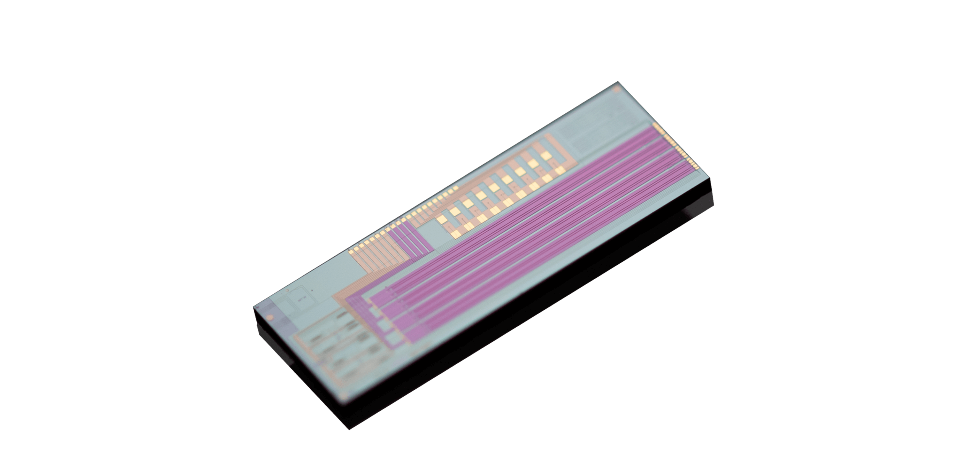
The buyer can review TFLN chips that include 800G, 1.6T, and 3.2T direct-detection options, a coherent PDMIQ device, and a bare high-speed die. They use these product categories to build a buyer checklist covering bandwidth, drive, loss, extinction, coupling, packaging, qualification, traceability, capacity, and lifecycle support.
Telecom Architecture Defines the Required Circuit Function
Buyers should begin by defining what the photonic integrated circuits must do. A DR4 or DR8 device provides multiple intensity-modulated lanes, while a coherent circuit creates balanced amplitude and phase paths.
They specify lane count, symbol rate, modulation format, polarization, laser arrangement, and receiver architecture before comparing bandwidth or voltage claims. For direct-detection programs, TFLN chips may reduce drive demand and support high rates, but multi-channel yield becomes important. They request lane-by-lane distributions, crosstalk, skew, extinction, and coupling data.
An integrated die that saves assembly steps can still raise module cost if one weak channel causes rejection or if final testing cannot isolate the failure mechanism. Coherent products introduce bias-control and balance requirements.
They examine path loss, quadrature error, linearity, differential phase, polarization handling, and large-signal behavior with the intended driver and DSP. The circuit should be assessed as part of a transmitter architecture, including controls and calibration, rather than compared with a simpler intensity modulator on raw insertion loss alone.
Data-Sheet Metrics Must Be Converted into Link and Module Margin
For telecom photonic integrated circuits, electro-optic bandwidth must support the waveform after packaging and board connection. They ask for test reference planes, response variation, and the frequency behavior of the delivered package.
The module team then measures with actual cables, launches, and drivers because a well-characterized bare-chip response may be reduced by interfaces outside the die. One direct-detection example among TFLN chips provides concrete figures: a 3.2T DR8 device at 110 GHz with differential half-wave voltage below 1.5 V, and a 1.6T DR8/800G DR4 device at 70 GHz with differential half-wave voltage below 2 V.
Their insertion-loss values include coupling, which helps their optical budget, but they still verify distribution and temperature behavior. For coherent formats, the 70 GHz PDMIQ option lists loss below 7 dB, differential half-wave voltage below 4.5 V, and extinction above 25 dB. They translate these figures into driver power, laser margin, expected OSNR, and link performance.
Device-level values become purchasing limits after correlation with a representative module and network test. They assess total landed cost through driver, laser, package, test, calibration, and expected yield, rather than treating chip price as the complete economic comparison.
Supplier and Packaging Controls Are Part of the Purchase
Commercial selection of photonic integrated circuits includes the package route. They identify who owns fiber coupling, RF transition, thermal design, mechanical tolerances, and reliability. Bare die may offer flexibility but requires more internal capability, while a packaged chip transfers responsibility to the supplier.
Contract terms should match the chosen integration boundary and failure-analysis process. TFLN chips also require statistical and lifecycle evidence. They review wafer capacity, lot traceability, screening, yield distribution, process-change notification, qualification status, and roadmap continuity.
Telecom products may remain deployed for years, so replacement compatibility and support after launch matter alongside current performance. A product change can trigger significant requalification across customers and systems. Incoming inspection and supplier quality plans are established before volume.
They agree on data fields, sampling, reference methods, and escalation thresholds. When results disagree, both parties need traceable calibration and shared samples. Clear technical ownership reduces disputes and prevents production interruptions while root cause moves among chip, package, module, and test organizations.
Roadmap reviews include standards and customer interoperability, so that a circuit optimized for one module format does not restrict future network compatibility. Buying a photonic circuit for telecom means buying an operating function, an integration route, and a manufacturing relationship.
Bandwidth, voltage, loss, and extinction are necessary parameters, but they gain commercial meaning after the chip is connected to the intended driver, laser, package, receiver, controls, and network requirement.
Their sourcing process moves from architecture requirements to sample characterization, packaged prototypes, multi-lot data, reliability work, and controlled production release. Procurement, engineering, quality, and operations participate together. This prevents price or one prominent specification from dominating a decision whose consequences extend through module yield and field service.
Telecom chip purchasing spans die data, package loss, driver demand, module yield, network margin, and supplier responsibility. Placing Liobate in that complete cost-and-risk model gives buyers a clearer basis for assigning integration work and interpreting module evidence.
